Powering High-Performance Image Sensors
七月 14, 2022
Share:

The power supply arrangement used with a CMOS image sensor can significantly affect its performance in terms of resolution, frame rate, etc. This blog considers some critical factors when designing a power supply solution for this application.
Inside a CMOS Image Sensor
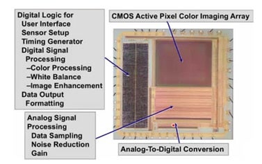
A typical CMOS imaging system includes an active pixel color array, analog signal processing circuitry, an analog-to-digital converter, and digital sections to control interfaces, timing, and data readout. The fill factor of the array is the percentage of photosensitive sections relative to the total size of the sensor. Photodetectors are light-sensitive transducers that gather and convert light photons into an electrical current (on the order of femtoamperes). Resolution is the term used to quantify the total number of pixels in a CMOS image sensor, with the pixels in a 2 MP sensor array, for example, arranged in 1600 columns and 1200 rows. However, not all pixels in an array are active (available for light detection) because some (optically black) pixels are for black level and noise correction purposes.

Figure 1: Typical CMOS Image Sensor Blocks
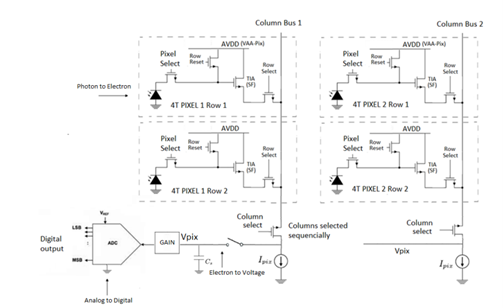
There are several different pixel transistor designs, including three (3T), four (4T), and five-transistor (5T) versions. In a 4T arrangement, photodiodes convert received light photons into an electrical charge. These tiny voltages are then read (one row at a time)—stored in a column capacitor (Cs). A decoder and multiplexer read the voltage stored in each column.

Figure 2: Four-Transistor Pixel Design
The frame rate, typically 30-120 fps, quantifies the speed at which an image array for processing captures a complete image. Frame rate is affected by shutter speed, which controls the time interval available for the image sensor to gather light. The programmable time interval, also called the dark period, when other tasks are performed after the last row has been read, also affects the frame rate, approximately 75% of the readout rate. Frame readout is performed row by row in a sequential fashion; at the end, a buffer stores the entire frame as a complete image.
Power Supply Design Considerations
CMOS image sensors typically use three different power rails - analog (2.8 V AVDD), interface (1.8 or 2.8 V DOVDD), and digital (1.2 or 1.8 V DVDD). A low voltage dropout (LDO) regulator with a large bypass capacitor on its input pin then stabilizes these supplies, helping to reduce voltage fluctuations and thereby improving the noise performance of the image sensor. The power supply rejection ratio (PSRR) measures how well an LDO can reject input voltage variations caused by mains ripple or noise generated by other switching regulators. An LDO with low PSRR can cause an unwanted horizontal ripple to be present in a captured image. It is possible to calculate the sensor row frequency required for a given frame rate before designing an LDO with sufficiently high PSRR for this application.

Figure 3: LDO Performing Voltage Regulation
The feedback loop inside an LDO largely determines the PSRR in systems operating at frequencies below 100 kHz. Still, for higher frequencies (above 100 kHz), passive components and PCB layout are the main contributors. Therefore, careful PCB design allows for tight current loops and reduces parasitic inductances. Basic LDOs have low values of PSRR at high frequencies. While this does not usually cause problems for standard cameras, higher resolution (50−200 MP) and high frame rate image sensors require an LDO with a PSRR over 90 dB at lower frequencies (up to 10 kHz) and greater than 45 dB at higher frequencies (1−3 MHz).
Design Tips
The frame rate (30−120 fps) and the row rate (22−44 kHz) create a dynamic load which causes under and overshoot on the analog rail. The current drawn appears like a step load at each new frame or row transition, meaning that during (or between) each frame and row read, an LDO must be able to handle load changes in the order of hundreds of milliamps. Bulk capacitors (with low impedance at the row and frame frequencies) can help with camera decoupling to reduce ripple caused by this load switching.
Each pixel in an image sensor has a charge saturation level (or a full well capacity)—the amount of charge a pixel can hold before saturation (measured in electrons) occurs. The dynamic range of an image sensor (specified in dB) is the ratio of the brightest and darkest parts of an image that can be captured simultaneously. Low spectral noise density (between 10 Hz to 1 MHz) at an LDO’s output also helps reduce the amount of noise transferred into the CMOS image sensor, thereby enabling a pixel to achieve a higher dynamic range. Finally, overall ripple and noise should be at least 40 dB below the noise threshold of a sensor, usually specified as the signal-to-noise ratio (SNR) on its datasheet.
Learn more in Majid’s white paper, Understanding Challenges in Powering High Resolution, High Frame Rate CMOS Image Sensors.