方案
By Technology
公司介绍
十月 28, 2024
Share:

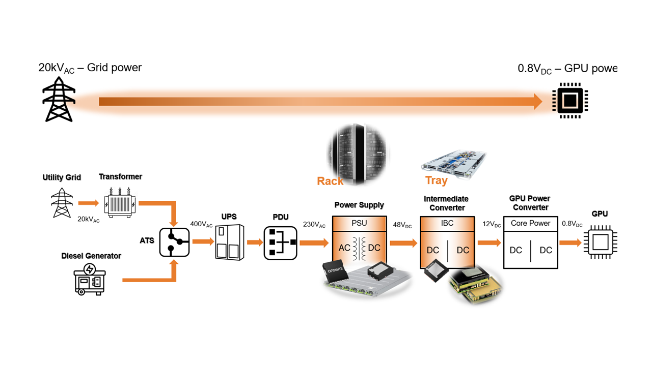
Today’s data centers need power semiconductors that efficiently convert electric power to reduce costs and lower emissions. More efficient power conversion equals less heat, which reduces cooling costs.
Power systems need lower total system cost and compact size; hence, higher power density – particularly as average power density in data centers is growing rapidly. This has increased from typically 5 kW per 1U rack a decade ago to 20 kW, 30 kW or more today.

Power supply units (PSUs) must also meet the specific needs of the data center industry. AI data center PSUs should meet the stringent Open Rack V3 (ORV3) base specification, requiring peak efficiency of over 97.5% from 30% to 100% load and minimum efficiency of 94% from 10% to 30% load.
As a key part of AC-DC conversion in PSUs, it’s essential to achieve high efficiency in the power factor correction (PFC) stage, which shapes the input current to maximize the ratio of useful power to total input power. PFC design is key in meeting electromagnetic compatibility (EMC) in regulations like IEC 61000-3-2 and ensuring compliance with energy efficiency specifications such as ENERGY STAR®.
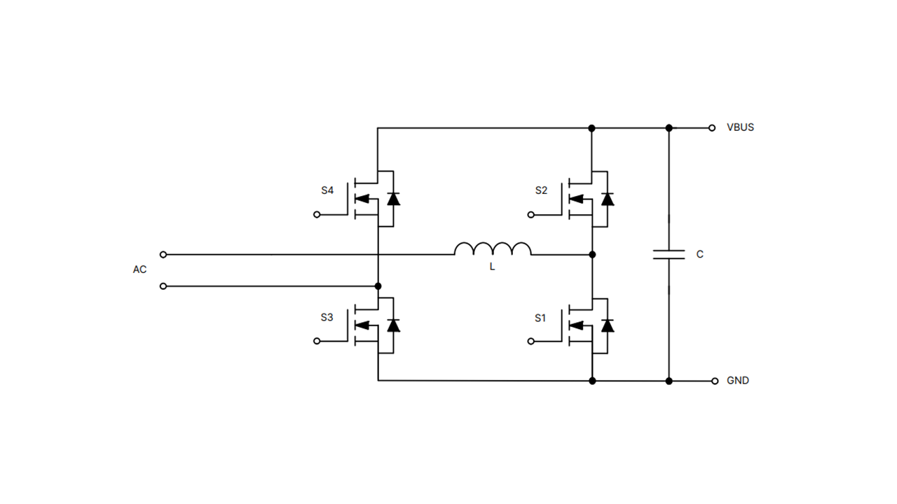
In many applications, the best approach is the “totem pole” PFC topology (Figure 2) typically used for the PFC block for 3 kW to 8 kW systems in data centers. Based on MOSFETs, totem pole PFC stages improve the efficiency and power density of AC power supplies by removing the bulky and lossy bridge rectifier.

To achieve 97.5% efficiency, a totem pole PFC requires MOSFETs using a “wide bandgap” semiconductor like silicon carbide (SiC). Today, all PFC stages use SiC MOSFETs for the fast-switching leg and silicon-based super junction MOSFETs for the phase or slow leg.
SiC MOSFETs have better performance and increased efficiency versus silicon (Si) MOSFETs such as super junction MOSFETs. They provide superior performance at high temperatures and better robustness and can operate at higher switching frequencies.
Compared to a Si MOSFET, a SiC MOSFET stores less energy in its output capacitance (EOSS), which is critical at low load conditions of PFC stages because the switching loss portion becomes major in whole MOSFET power dissipation at low load operation. Lower EOSS and gate charge minimizes energy losses in switching, thus enabling higher efficiency in the totem pole PFC fast leg. Also, a SiC MOSFET displays better (positive) temperature co-efficient of RDS(ON) compared to a Si MOSFET because of its superior thermal conductivity, which is three times better than silicon-based devices.
This means that on-resistance increases less with a rise in junction temperature for a SiC MOSFET than for a Si MOSFET. At high temperatures such as 175ºC, the SiC MOSFET has lower conduction losses that dominate the overall power loss.
The table below shows the key parameter comparison of currently available 650V super junction MOSFET and onsemi’s 650V SiC MOSFET.
BVDSS | Technology | RDS(ON) (Typ.) @TJ:25C | RDS(ON) (Typ.) @TJ:175C | Qg@400V | Eoss @400V |
| 650 V | Super junction MOSFET | 23 mohm | 57.5 mohm | 259 nC | 27 uJ |
| 650 V | M3S SiC MOSFET | 23 mohm | 34.5 mohm | 69 nC | 15 uJ |
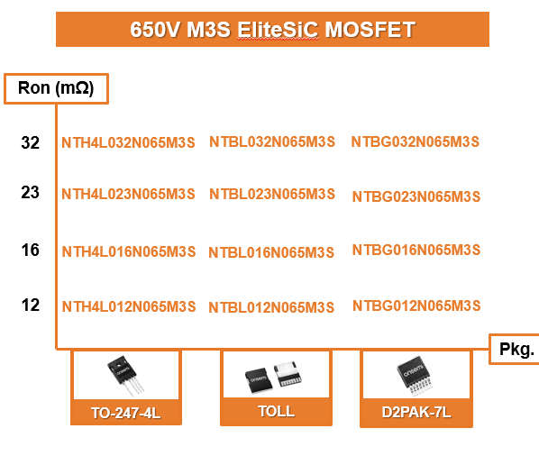
Among other SiC MOSFET options, the 650 V M3S EliteSiC MOSFETs from onsemi, including the NTBL032N065M3S and NTBL023N065M3S, provide best-in-class switching performance and significantly improve PFC and LLC stage efficiency in hyperscale data centers.
M3S EliteSiC technology surpasses its predecessor with a 50% lower gate charge, 44% lower EOSS, and 44% less stored charge in its output capacitance (QOSS). This superior EOSS figure improves system efficiency at light loads when used in a hard switching topology in the PFC stage. Additionally, lower QOSS simplifies resonant tank inductance design for soft-switching topologies in the LLC stage.
M3S EliteSiC MOSFETs dissipate less heat thanks to excellent switching performance and power efficiency. Additionally, the gate charge Qg of the MOSFETs is one of the best in this voltage class, to reduce gate drive losses. Excellent Qgs and Qgd also reduce switching turn-on and turn-off losses.

In the LLC block, the VDS transition from off-state to diode conduction requires discharging the output capacitance. To achieve this quickly, low transient output capacitance is necessary. Transient COSS is important as this minimizes the circulating losses from the resonant tank and allows for shorter dead time for the LLC, resulting in reduced circulating losses on the primary side. A low resistance in the on-state minimizes conduction losses, and a low EOFF helps minimize switching.
Overall, higher system efficiency is the most important performance criterion, which makes SiC MOSFETs an optimal choice in data center PFC and LLC stages.
Among other SiC MOSFETs in the market, onsemi’s 650V EliteSiC MOSFETs are competitive against super junction MOSFETs in terms of cost, EMI, high-temperature operation, and switching performance based on the same RDS(ON). The 650V M3S EliteSiC MOSFET approaches lower RDS(ON) than super junction MOSFETs in the same package, which improves system efficiency in LLC topology, and it scores highly over silicon alternatives due to its much lower switching losses.

Learn more about onsemi’s 650V EliteSiC MOSFETs
Watch this video to learn more about how our technologies empower demanding hyperscale centers.