方案
By Technology
公司介绍
五月 18, 2023
Share:

While efficiency and size are two of the primary considerations in the design of power supplies, Power Factor Correction (PFC) is also becoming increasingly important. PFC is required to minimize the impact of power supply operation on the AC mains infrastructure by reducing the amount of harmonic content on power lines and losses due to reactive power. However, designing a low-footprint, highly-efficient power supply, including PFC, is challenging. This blog shows how modifying a conventional PFC topology can help achieve this.
A bridge rectifier followed by a single-phase PFC stage, consisting of four rectifier diodes and one boost diode, is commonly used at the input stage of a power supply.

An alternative approach that can be used to improve power supply efficiency is to use a totem pole topology that removes the bridge rectifier and replaces the boost diode with a fast−switching MOSFET. To understand how this can be done, it helps to first think of this topology as combining the functionality of two separate boosts circuits - one for each half-cycle of the input sinusoidal waveform.
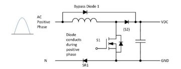
An inductor, capacitor, MOSFET S1, and diode (S2) operate as a positive boost circuit on the positive half cycle. In addition, a bypass diode is included to prevent the inductor from saturating at start−up or under abnormal operating conditions, and a protection diode (SR1) prevents operation during the negative half cycle.
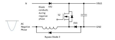
For the negative half cycle, the inductor, capacitor, MOSFET S2, and diode (S1) form an inverted version of the standard boost circuit with an additional protection diode SR2 in the on−state current pathway.
In the totem pole PFC topology, the two diodes (SR1 and SR2) can be replaced by MOSFETs to achieve higher efficiency. This is because they conduct during the operation of the totem pole but switch only at 50/60 Hz. The bypass diodes only conduct at start−up, so there is no benefit from replacing them with MOSFETs.
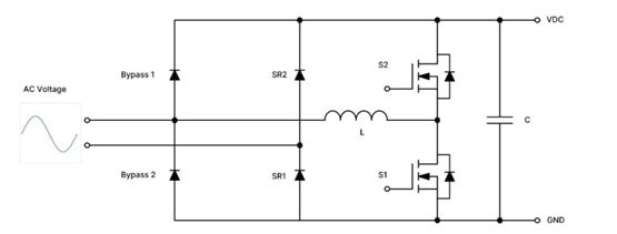
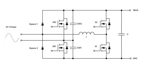
A modified totem pole PFC topology uses a combination of fast SiC MOSFETs and slow super-junction MOSFETs. During the positive half wave, SR1 is switched on for the whole cycle and provides the path ground path for the asynchronous boost circuit. S1 acts as a boost switch, while S2 performs the diode function in an asynchronous boost. Similarly, during the negative half cycle, SR2 provides the ground path with S2 as the boost switch and S1 acting as a diode in asynchronous boost. SR1 and SR2 can be low−speed super-junction MOSFETs (since they are only required to switch at low frequencies). To prevent potential EMI problems, additional capacitors are needed to avoid the zero-crossing transition from happening too quickly. However, if the capacitor values are too large, the total harmonic distortion (THD) performance will worsen. For high power density, S1 and S2 can be SiC devices.
onsemi used a high−frequency PFC front end with EliteSiC switches, an advanced totem−pole PFC controller, and a high−frequency LLC stage running up to 150 kHz using high−speed synchronous rectification on the output stage to design a single−phase AC input 3 kW PFC power supply with a power density of over 40 W/in3 and full load efficiency of 98.4%. The operation and performance of this innovative solution are described in detail in a white paper available to download here.
You need a reliable SiC partner to accomplish your product development and growth objectives. That partner should have a leading edge technology roadmap, and a proven reputation for product performance. After all, maintaining control over supply, quality, cost, efficiency and supply chain is challenging with SiC.